Recently, the latest research achievement of Assoc Professor Hu Huan of ZJUI and his team, titled "Atomic Force Microscope (AFM) Nanospherical Probe", was officially published in the internationally renowned journal Nanoscale. In collaboration with Professor Xu Yang from Zhejiang University, Assoc Professor Hu Huan led the team to develop a cleaning technology based on the nanospherical atomic force microscope (AFM) probe, which can achieve the cleaning of the heterojunction interface of two-dimensional materials with almost no damage. Ding Xiaolei, a doctoral student at Zhejiang University, is the first author of the article, and the corresponding authors are Assoc Professor Hu Huan from ZJUI and Professor Xu Yang from Zhejiang University.
Van der Waals heterojunction technology lies at the heart of post - Moore era electronic devices, boasting vast application prospects. The van der Waals heterojunction of two - dimensional materials is crafted through the precise stacking of diverse two - dimensional materials with distinct properties, much like assembling atomic - level building blocks. By deftly tuning crucial parameters, similar to adjusting the knob of a precision instrument, the performance of the device can be efficiently regulated and reengineered.
However, in the critical stages of preparation and transfer, the material surface is highly susceptible to contamination. Bubbles mixed in during preparation, residual polymers during transfer, and various impurities act as hidden troublemakers, disrupting the tight coupling between layers and affecting the excellent performance of the material.
Two dimensional materials are like a thin and delicate 'nano canvas', while pollutants are like droplets on the canvas, affecting their intrinsic properties and hindering subsequent functional implementation. So the research team believes that how to efficiently and non destructively remove these pollutants and restore the pure color of this "nano canvas" has become an important challenge facing this technology.
At present, probe contact mode cleaning technology based on atomic force microscopy (AFM) has become an important tool for surface cleaning of two-dimensional materials. However, its cleaning method is more like a "carving knife": applying high-intensity pressure through a very small contact area can remove some stains, but it is extremely easy to leave scratches on the material surface, and even cause irreversible damage, especially when cleaning large bubbles or stubborn pollutants.
To break through the limitations of traditional probes, the research team has developed a brand-new Nano-Spherical Probe. Assoc Prof. Hu Huan told us, “in contrast to the "graver-style" cleaning of traditional pyramid probes, the Nano-Spherical Probe is more like a ‘paintbrush’. Through uniform and gentle contact, it sweeps away the contaminants from the ‘canvas’, while protecting the structural integrity of the two-dimensional materials. ”

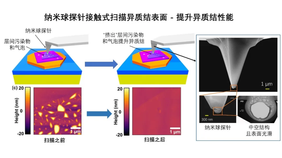
Schematic diagram of nanosphere probe
It is worth noting that the nano spherical probe demonstrated superior performance in the application experiment on molybdenum disulfide/hexagonal boron nitride (MoS ₂/hBN) samples, effectively removing pollutants on the surface of two-dimensional materials and significantly improving optical uniformity. In addition, the detection results of Kelvin Probe Force Microscopy (KPFM) further confirm that the uniformity of the material's potential distribution is not affected after the cleaning process, indicating that the nanosphere probe not only efficiently removes pollutants, but also has significant advantages in maintaining the integrity of the material's surface morphology and electrical stability.

(a) (b) Schematic diagram of scanning two-dimensional material heterojunctions with nanosphere probes, (c) (d) AFM images of MoS ₂/hBN before and after cleaning with nanosphere probes, (e) SEM images of nanosphere probes and internal composition maps of small spheres.
Therefore, the research team has concluded that nanosphere probe technology can effectively optimize the interface of electronic devices, remove surface pollutants, and suppress the generation of defects by precisely regulating the contact force and pressure distribution. On this basis, the research team plans to focus on the interface between graphene and silicon, as well as devices such as transition metal sulfide field-effect transistors (FETs).
By conducting more in-depth experimental verification and optimization work, we strive to achieve substantial breakthroughs in key performance indicators such as improving electron transfer efficiency, reducing switch threshold, and increasing carrier mobility, "said Ding Xiaolei, a member of the research group.
This research achievement will not only significantly improve the performance and reliability of electronic devices, but also has the potential to reshape the application pattern of two-dimensional materials in multiple fields such as electronics, energy, and communication worldwide, opening up an unprecedented new path for the digital transformation and technological leap of human society.
Article Link:https://pubs.rsc.org/en/Content/ArticleLanding/2025/NR/D4NR03583F


